
Best 4 Inch SiC Substrate (4H-N Type) Low-Resistivity SiC Wafer Supplier
High-quality 4-inch SiC substrate manufacturer with 4H polytype, N-type Nitrogen doping and ultra-low resistivity (0.015–0.028 Ω·cm). Ideal for power ...
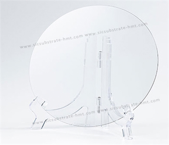
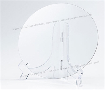
HMT's 4'' Silicon Carbide (SiC) substrates are engineered to deliver exceptional performance in high-power, high-frequency, and high-temperature environments. Featuring a 4H polytype structure with N-type nitrogen doping, these substrates achieve ultra-low resistivity (0.015–0.028 Ω·cm) – making them ideal for next-generation power electronics, RF devices, and LED applications. We offer competitive pricing for semiconductor companies, research laboratories, and academic institutions seeking high-value SiC solutions.
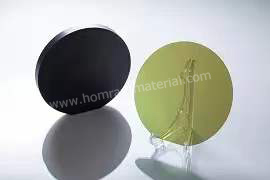 HMT SiC Substrate Product Range
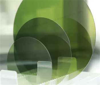
2inch 4 inch 6 inch 8 inch SiC Substrate Wafers
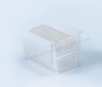
2inch 4 inch 6 inch 8 inch SiC As-cut Wafers
2inch 4 inch 6 inch 8 inch Single Crystal SiC Boules
4 inch 6 inch 8 inch SiC on SiC Epi Wafer
Key Specifications:
Diameter: 100±0.25 mm | Thickness: 350μm±25μm
Grade Options: D / R / P (Device, Research, Production)
Orientation: 4.0° off-axis toward <1120>±0.5°
Surface Finish: Si-face Chemical Mechanical Polishing (CMP) for atomically smooth surfaces.
Back Finish: C-face polished to enhance handling and integration.
Primary Flat: (1-100)±5.0° orientation | Flat Length: 32.5 mm±2 mm
Applications:
Power devices (MOSFETs, IGBTs)
RF and microwave components
High-brightness LEDs
Automotive and aerospace semiconductors
Why Choose Our SiC Substrate?
Consistent Quality: Tight tolerances on thickness, diameter, and orientation ensure reliable performance.
Advanced Processing: CMP-polished surfaces minimize defects and optimize epitaxial layer deposition.
Versatility: Suitable for R&D, prototyping, and mass production across industries.
Optimized for seamless integration into cutting-edge semiconductor workflows, our 4-inch SiC substrate sets the standard for durability, efficiency, and scalability. Contact us to customize specifications for your project needs.
CATEGORIES
LATEST NEWS
- Introduction to the main functions of PbootCMS
What Is a TCB Nozzle? Materials, Vacuum Holding and SiC Nozzle Manufacturing
- Introduction to the main functions of PbootCMS
SiC : Industrial Ceramic vs Semiconductor Applications
- Introduction to the main functions of PbootCMS
How Does AI Help Singe Crystal SiC Boule Growth
- Introduction to the main functions of PbootCMS
Technical Analysis of SiC Wafer For Power Semiconductor Devices in New Energy Vehicles
CONTACT US
Contact: Mr.Kimrui
Phone:
Tel: Please send your detailed inquiry or requirements via email below.
Email: kim@homray-material.com
Add: Please send your detailed inquiry or requirements via email below.