6 inch SiC Wafer Manufacturer For MOSFET
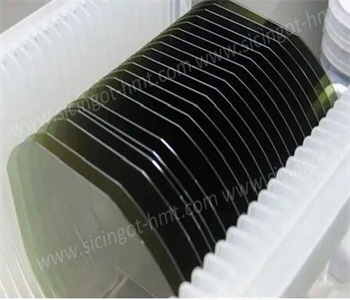
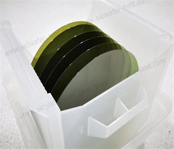
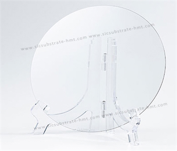
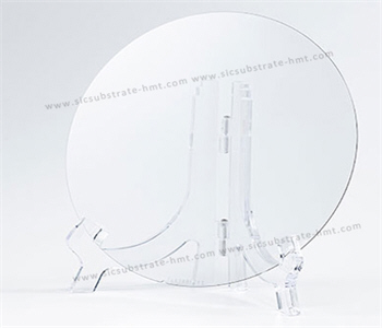
SiC Wafers can be used as substrate for SiC on SiC Epitaxy wafer, HMT offer 6 inch ultra low MPD SiC Wafer for MOSFET semiconductor device fabrication...
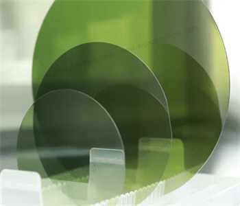
SiC Wafers can be used as substrate for SiC on SiC Epitaxy wafers, HMT offers 6 inch ultra low MPD<0.2cm2 SiC Wafer for MOSFET semiconductor device fabrication. Normally,we supply 6 inch and 8 inch SiC wafers, but if customers have 2 inch or 4 inch SiC Wafers demand, we can make special produciton for them. Production Grade 6 inch SiC wafer for MOSFET the MPD<0.2cm2 ohter parameters also mucm better than D grade SiC wafers. Please don't worried about cost, we always provide best price for customers.
Q: SiC Wafer Dimension ?
A: We can supply 2 inch 4 inch 6 inch 8 inch SiC Wafers.
Q: What grade of SiC Wafer in HMT company?
A: We have D grade R grade and P grade SiC Wafer for different application.
Q: If customer need customization, can HMT support this?
A: Of course, we support customized SiC Wafer upon different spec.
Q: Leadtime for SiC Wafers
A: Normally leadtime is within 4 weeks,we'll confirm the leadtime before sign the contract.
Q: Transportation way
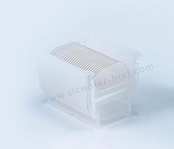
A: We use safety casssette to package SiC Wafers and delivery by FedEx,DHL etc.
CATEGORIES
LATEST NEWS
- Introduction to the main functions of PbootCMS
What Is a TCB Nozzle? Materials, Vacuum Holding and SiC Nozzle Manufacturing
- Introduction to the main functions of PbootCMS
SiC : Industrial Ceramic vs Semiconductor Applications
- Introduction to the main functions of PbootCMS
How Does AI Help Singe Crystal SiC Boule Growth
- Introduction to the main functions of PbootCMS
Technical Analysis of SiC Wafer For Power Semiconductor Devices in New Energy Vehicles
CONTACT US
Contact: Mr.Kimrui
Phone:
Tel: Please send your detailed inquiry or requirements via email below.
Email: kim@homray-material.com
Add: Please send your detailed inquiry or requirements via email below.