

8'' HPSI SiC Wafer AR+AI
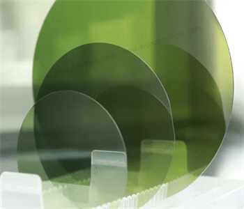
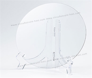
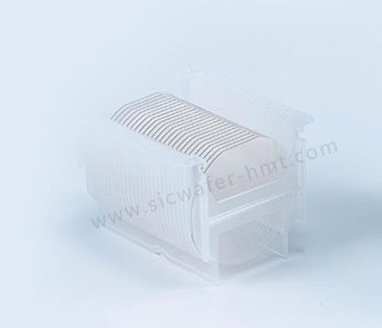
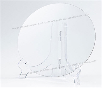
8'' HPSI SiC Wafer(AR+AI) Manufacturer HMT supply 200mm large size semi-insulating SiC Wafer for AR glasses application. we also offering customizatio...
8'' HPSI SiC Wafer(AR+AI) Manufacturer HMT supply 200mm large size semi-insulating SiC Wafer for AR glasses application. We have both D grade and P grade of HPSI SiC Wafers. What'more, HMT can manufacture any customized Conductive N type SiC wafer thickness like 500um, 800um etc with very preferential price for all customers.
Key Advantages of HPSI SiC Wafers
● High Refractive Index (approximately 2.6): Enables more efficient light guidance in AR optical waveguide systems, reducing optical loss by 30% compared to glass materials, and supports more compact optical designs.
● High Transmittance: SiC material exhibits high transmittance in the visible and near-infrared spectrum (400nm-1100nm), making it particularly suitable for AR optical waveguide systems. It significantly reduces optical loss, improves image brightness, and enhances immersion.
● High Thermal Conductivity: Efficiently dissipates heat from electronic components, effectively addressing issues such as wearing discomfort and lifespan degradation caused by device overheating.

CATEGORIES
LATEST NEWS
- Introduction to the main functions of PbootCMS
What Is a TCB Nozzle? Materials, Vacuum Holding and SiC Nozzle Manufacturing
- Introduction to the main functions of PbootCMS
SiC : Industrial Ceramic vs Semiconductor Applications
- Introduction to the main functions of PbootCMS
How Does AI Help Singe Crystal SiC Boule Growth
- Introduction to the main functions of PbootCMS
Technical Analysis of SiC Wafer For Power Semiconductor Devices in New Energy Vehicles
CONTACT US
Contact: Mr.Kimrui
Phone:
Tel: Please send your detailed inquiry or requirements via email below.
Email: kim@homray-material.com
Add: Please send your detailed inquiry or requirements via email below.