SiC Substrate Producer 4H 100mm Silicon Carbide Wafer 150dia
HMT supplies 4H-SiC substrates (100/150/200mm) for semiconductor chips. Choose conductive/semi-insulating types & P/R/D grades. Foundation-grade mater...
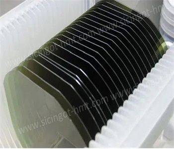
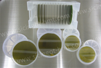
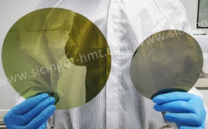
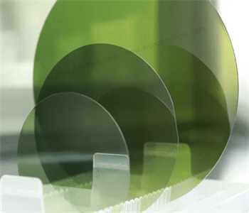
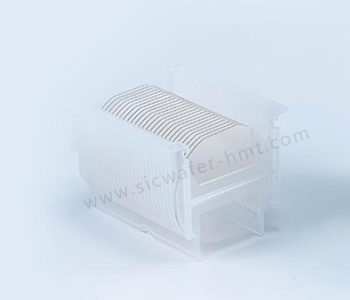
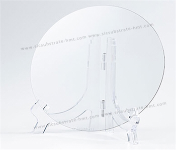
Homray Material Technology (HMT) supplies 4H-SiC substrates in three industry-standard diameters: 100mm, 150mm, and 200mm. Available in both conductive and semi-insulating types, these substrates offer flexible grading options (P-grade, R-grade, or D-grade) tailored to specific project requirements.
When SiC is utilized as the substrate material, production costs are typically higher due to its superior material properties, positioning HMT's solutions as high-value components for advanced semiconductor applications.Silicon carbide (SiC) substrates form the critical foundation of semiconductor chips, analogous to a building's structural base.
Substrate materials have now evolved to the third generation , but the relationship between generations is not one of replacement. Instead, each generation is applied in different fields due to their distinct properties.
First-generation substrates are primarily silicon-based For example, CPUs and GPUs use silicon substrates, and currently, 90% of semiconductor substrates are made of silicon (used in large-scale integrated circuits ).
Second-generation substrates are represented by indium phosphide (InP) and gallium arsenide (GaAs) . Due to their high-speed, high-frequency optoelectronic properties, they are mainly used in optical modules, LEDs, and optoelectronic devices (e.g., **optical communication, optical display, and optical storage ).
Third-generation substrates include silicon carbide (SiC) and gallium nitride (GaN) . Thanks to their high-temperature and high-voltage resistance, they are primarily used in new energy vehicles, photovoltaics, and other fields (for high-frequency, high-power electronic devices ).
 Coexistence and Synergy of the Three Generations of Semiconductors
Complementarity, Not Replacement :
Silicon remains the absolute mainstream for logic chips and consumer electronics (accounting for 95% of the global semiconductor market ).
GaAs and InP dominate high-frequency and optoelectronic niche markets .
SiC/GaN play an irreplaceable role in new energy and industrial applications .
Examples of Technological Integration :
GaN-on-Si: Combining gallium nitride with low-cost silicon substrates for fast charging and RF applications
iC-IGBT hybrid modules : Integrating silicon carbide with IGBTs to improve power grid conversion efficiency .
Future Trends:
Heterogeneous integration: Combining different materials (e.g.,Si + GaN) on a single chip to balance performance and cost.
Ultra-wide bandgap materials: Emerging materials like gallium oxide (Ga₂O₃) and diamond may unlock new applications in ultra-high voltage (beyond 20kV) and quantum computing.

CATEGORIES
LATEST NEWS
- Introduction to the main functions of PbootCMS
SiC : Industrial Ceramic vs Semiconductor Applications
- Introduction to the main functions of PbootCMS
How Does AI Help Singe Crystal SiC Boule Growth
- Introduction to the main functions of PbootCMS
Technical Analysis of SiC Wafer For Power Semiconductor Devices in New Energy Vehicles
- Introduction to the main functions of PbootCMS
SiC industry is stepping into 8 inch with 12 inch substrates making accelerated breakthroughs
CONTACT US
Contact: Mr.Kimrui
Phone:
Tel: Please send your detailed inquiry or requirements via email below.
Email: kim@homray-material.com
Add: Please send your detailed inquiry or requirements via email below.