
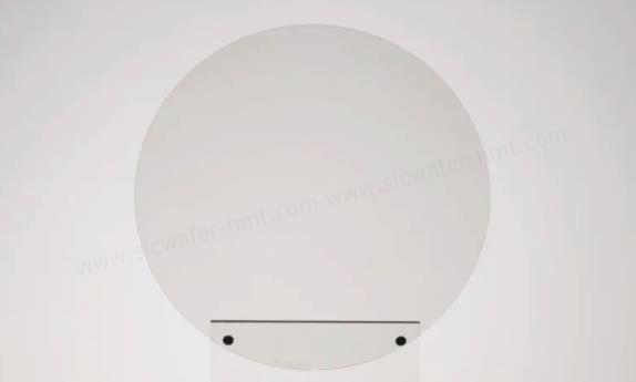
6-Inch Un-doped HPSI SiC Wafers for GaN RF
6 inch SiC wafer, HPSI SiC substrate, semi-insulating silicon carbide, GaN-on-SiC wafer, RF SiC wafer, 150mm SiC supplier, high resistivity SiC, HMT S...
6-Inch Un-doped HPSI SiC Wafers for GaN RF & Power Electronics
Product Overview
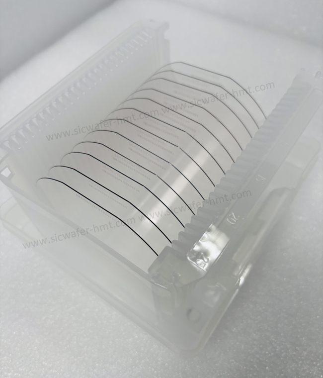
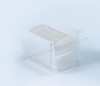
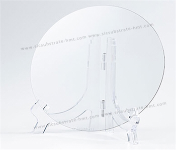
HMT is a professional manufacturer of silicon carbide (SiC) wafers, offering high-quality 6-inch (150mm) Un-doped High-Purity Semi-Insulating (HPSI) SiC substrates. With resistivity exceeding 10^8 Ω·cm, our HPSI wafers meet the stringent requirements of advanced RF and power applications.
Key Specifications
Diameter: 150mm (6 inch)
Type: Un-doped HPSI (High-Purity Semi-Insulating)
Resistivity: >10^8 Ω·cm
Crystal Structure: 4H-SiC
Surface Finish: Double-side polished (DSP)
Surface Roughness: ≤0.2nm
Thickness: 500 μm ± 25 μm
TTV (Total Thickness Variation): ≤ 8 μm
Bow/Warp: ≤ 30 μm
Primary Applications
1. GaN RF Devices (5G & Radar)
Our HPSI SiC substrates are the ideal platform for growing high-quality GaN epitaxial layers. The resulting GaN-on-SiC epi wafers are processed into HEMTs (High Electron Mobility Transistors) for 5G base stations, military radar, and satellite communication systems.
2. Power Electronics (EVs & Industrial)
For conductive (N-type) SiC wafers, applications include Schottky diodes, MOSFETs, and IGBTs used in electric vehicles (EVs), rail transportation, and high-power transmission systems.
Why Choose HMT?
Manufacturer Direct: Competitive pricing with full quality control
Customization: Available in various diameters (2", 4'',6", 8") and specifications
Global Shipping: Reliable logistics to North America, Europe, and Asia
Related Products
CATEGORIES
LATEST NEWS
- Introduction to the main functions of PbootCMS
What Is a TCB Nozzle? Materials, Vacuum Holding and SiC Nozzle Manufacturing
- Introduction to the main functions of PbootCMS
SiC : Industrial Ceramic vs Semiconductor Applications
- Introduction to the main functions of PbootCMS
How Does AI Help Singe Crystal SiC Boule Growth
- Introduction to the main functions of PbootCMS
Technical Analysis of SiC Wafer For Power Semiconductor Devices in New Energy Vehicles
CONTACT US
Contact: Mr.Kimrui
Phone:
Tel: Please send your detailed inquiry or requirements via email below.
Email: kim@homray-material.com
Add: Please send your detailed inquiry or requirements via email below.