8 inch Conductive 4H-N type SiC Wafer Supplier
Explore HMT's premium 2-8 inch SiC wafers with N-type/SI-type options. Discover semi-insulating & conductive substrates for GaN RF devices in 5G, rada...
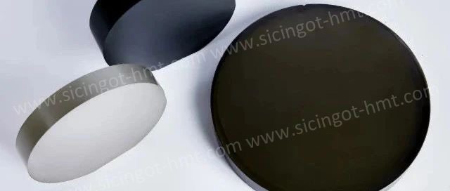
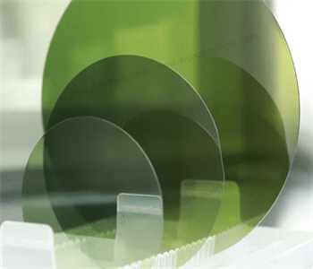
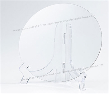
SiC Wafers are revolutionizing semiconductor manufacturing with their superior thermal conductivity, high voltage tolerance, and energy efficiency. At HMT, we specialize in producing advanced 2'' (50mm), 4'' (100mm), 6-inch (150mm), and 8-inch (200mm) SiC wafers, driving the industry shift toward large-diameter 12'' SiC substrates for enhanced productivity and cost efficiency.
SiC Wafer Types: Semi-Insulating vs. Conductive
1️⃣ Semi-Insulating SiC Wafers
Resistivity: >1e5 Ω·cm via ultra-high purity crystal growth
Applications:
GaN RF devices for 5G/6G base stations (3-6 GHz bands)
Military-grade radar systems (X-band to Ka-band)
Satellite communication power amplifiers
2️⃣ Conductive SiC Wafers
Doping: Nitrogen-doped for <0.02 Ω·cm resistivity
Applications:
EV power modules (900V+ SiC MOSFETs)
Industrial motor drives
Solar inverter systems
Gallium nitride RF devices prepared with semi-insulated SiC substrate are mainly power amplifiers for communication base stations and radar applications. Gallium nitride RF devices are the most ideal microwave RF devices so far, so it has become the core microwave RF devices in 4G/5G mobile communication systems, a new generation of active phased array radar and other systems.
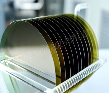
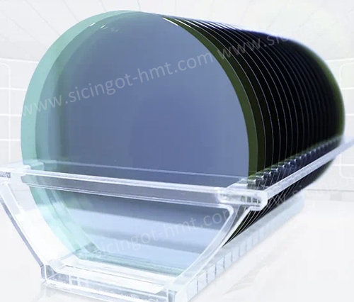
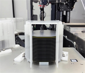
8 inch SiC Substrae wafer and 8 inch SiC Boule Pictures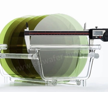

CATEGORIES
LATEST NEWS
- Introduction to the main functions of PbootCMS
SiC : Industrial Ceramic vs Semiconductor Applications
- Introduction to the main functions of PbootCMS
How Does AI Help Singe Crystal SiC Boule Growth
- Introduction to the main functions of PbootCMS
Technical Analysis of SiC Wafer For Power Semiconductor Devices in New Energy Vehicles
- Introduction to the main functions of PbootCMS
SiC industry is stepping into 8 inch with 12 inch substrates making accelerated breakthroughs
CONTACT US
Contact: Mr.Kimrui
Phone:
Tel: Please send your detailed inquiry or requirements via email below.
Email: kim@homray-material.com
Add: Please send your detailed inquiry or requirements via email below.