
Semi-insulating SiC Boule Supplier
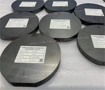
We manufacture6'' high-purity semi-insulating (HPSI) SiC bouleswith preciseon-axis orientation (<0001> ±0.2°). Available in two speciali...
We manufacture 6'' high-purity semi-insulating (HPSI) SiC boules with precise on-axis orientation (<0001> ±0.2°). Available in two specialized grades: D-grade boules for process development (laser cutting, cold splitting, water-jet laser slicing, and wire saw qualification). P-grade boules for volume production.
As the most mature third-generation semiconductor material, SiC enables critical applications across new energy vehicles, high-speed rail, aerospace, and 5G/wireless communications – truly becoming the 'silicon carbide for everything'.
Contact us for custom boule specifications and competitive quotations.
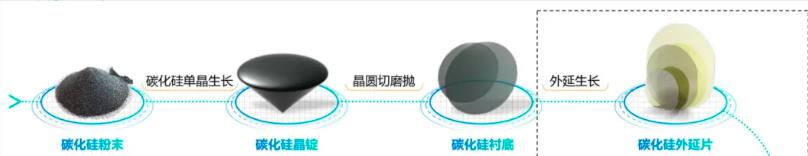
From the point of view of the process flow, SiC is generally first made into a crystal boule, and then through slicing, grinding, polishing to obtain silicon carbide substrate; Epitaxial substrate is grown to obtain epitaxial sheet. The epitaxial sheet is made into a device through the steps of photolithography, etching, ion implantation, deposition, etc., and the device is assembled into a module in a special shell.
The key equipment for SiC Boue growth and processing includes:
SiC powder synthesis equipment,
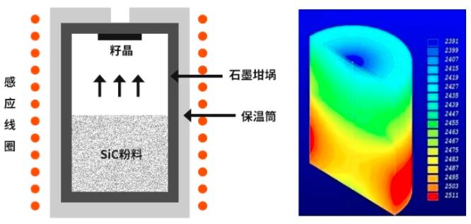
SiC single crystal growth furnace
Diamond multi-line cutting machine
SiC grinding machine
SiC polishing machine, etc.
SiC single crystal is extremely rare in nature, almost does not exist, can only rely on artificial synthesis. The preparation methods of silicon carbide ingot are divided into physical vapor transfer (PVT), chemical vapor deposition and liquid phase epitaxy.
At present, the most mature commercial method is the physical gas phase transmission method, which is also the method to achieve industrial large-scale production. This method needs to sublimate the powder under high temperature vacuum environment, and then through the control of temperature field, let the sublimed components grow on the surface of the seed crystal to obtain silicon carbide crystal.

CATEGORIES
LATEST NEWS
- Introduction to the main functions of PbootCMS
SiC : Industrial Ceramic vs Semiconductor Applications
- Introduction to the main functions of PbootCMS
How Does AI Help Singe Crystal SiC Boule Growth
- Introduction to the main functions of PbootCMS
Technical Analysis of SiC Wafer For Power Semiconductor Devices in New Energy Vehicles
- Introduction to the main functions of PbootCMS
SiC industry is stepping into 8 inch with 12 inch substrates making accelerated breakthroughs
CONTACT US
Contact: Mr.Kimrui
Phone:
Tel: Please send your detailed inquiry or requirements via email below.
Email: kim@homray-material.com
Add: Please send your detailed inquiry or requirements via email below.