Custom Thickness SiC Wafers Manufacturer | 2"-8" Sizes | SiC Finishing Parts
Semiconductor wafer manufacturing-HMT Company specializes in producingnonstandard As-Cut SiC wafers(Unpolished SiC Wafers)to your unique specification...
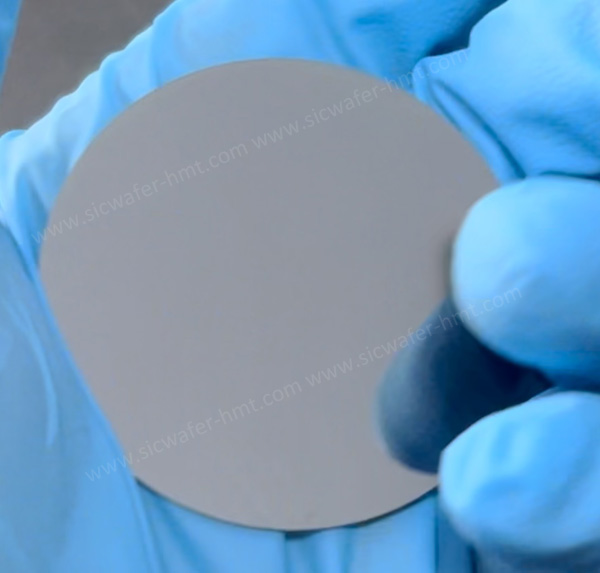
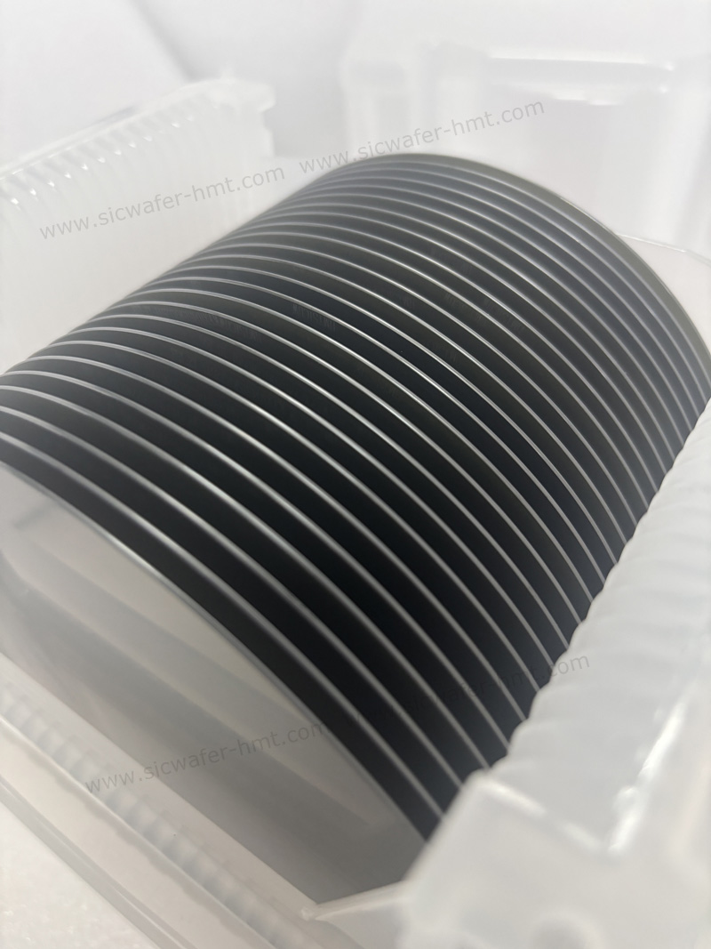
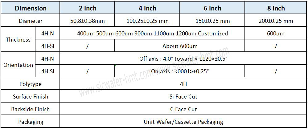
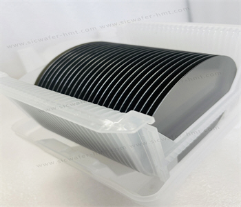
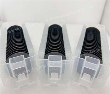
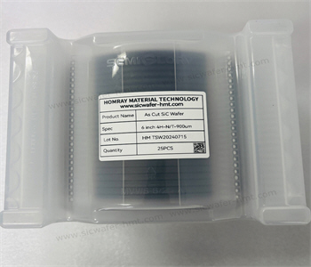
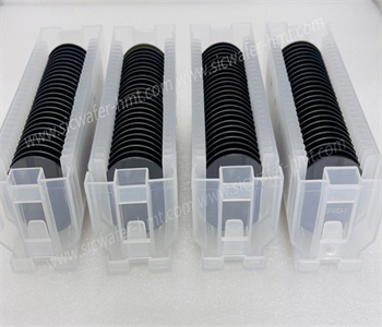
Semiconductor wafer manufacturing-HMT Company specializes in producing nonstandard As-Cut SiC wafers(Unpolished SiC Wafers)to your unique specifications. Unlike most manufacturers limited to standard thicknesses (e.g., 350µm or 500µm), we offer customizable thicknesses ranging from 500µm to 1600µm, including 600µm, 900µm, 1100µm, and 1600µm options. Our unprocessing SiC wafers are available in all standard dimensions (2-inch, 4-inch, 6-inch, and 8-inch) to meet diverse industrial needs. Whether you require standard SiC Substrate or nonstandard SiC Raw-cut wafers, HMT guarantees competitive pricing without compromising quality.
Product Applications:
HMT’s ultra-thick SiC wafers (up to 1600µm) are ideal for demanding applications such as:
High-power semiconductor devices
Electric vehicle (EV) power electronics
Renewable energy systems (solar inverters, wind turbines)
Aerospace and defense electronics
High-temperature and radiation-resistant components
Their robust thickness enhances durability and performance in extreme environments, making them perfect for R&D and industrial prototyping.
In recent years, SiC has become an important player in the semiconductor industry, powering MOSFETs, Schottky diodes, and power modules for high-power, high-efficiency applications. SiC is more expensive than silicon MOSFETs (silicon MosFETs are typically limited to a breakdown voltage of 900V), but SiC can achieve voltage thresholds close to 10kV.
SiC also has extremely low switching losses and is able to support high operating frequencies, resulting in today's unparalleled efficiency, especially in applications with operating voltages exceeding 600 volts. When implemented properly, SiC devices can reduce converter and inverter system losses by nearly 50%, reduce size by 300%, and reduce overall system costs by 20%. The reduction in overall system size makes SiC useful in weight - and space-sensitive applications.
CATEGORIES
LATEST NEWS
- Introduction to the main functions of PbootCMS
SiC : Industrial Ceramic vs Semiconductor Applications
- Introduction to the main functions of PbootCMS
How Does AI Help Singe Crystal SiC Boule Growth
- Introduction to the main functions of PbootCMS
Technical Analysis of SiC Wafer For Power Semiconductor Devices in New Energy Vehicles
- Introduction to the main functions of PbootCMS
SiC industry is stepping into 8 inch with 12 inch substrates making accelerated breakthroughs
CONTACT US
Contact: Mr.Kimrui
Phone:
Tel: Please send your detailed inquiry or requirements via email below.
Email: kim@homray-material.com
Add: Please send your detailed inquiry or requirements via email below.