

100mm 4 inch SiC Wafer Manufacturer 4H-N Type
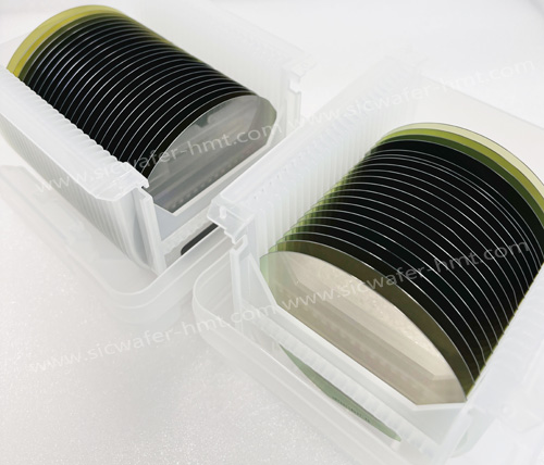
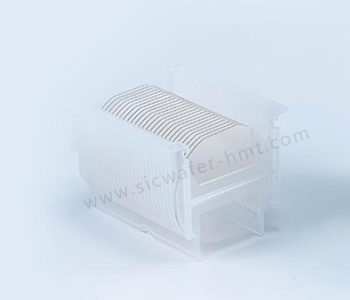
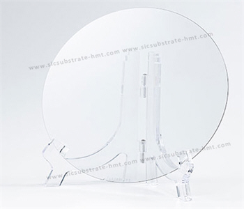
HMT supplies high-quality 4-inch (100mm) 4H-N conductive SiC wafers with resistivity 0.015-0.028 Ω·cm. Ideal for SiC diodes, MOSFETs, and power module...
4H-N Conductive SiC Wafers | 4-Inch N-Type Substrates for Power Electronics
Product Overview
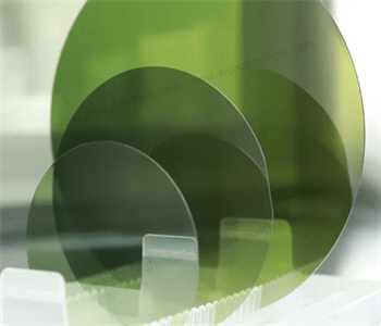
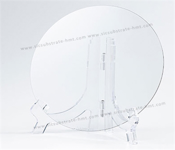
HMT Semiconductors is a professional manufacturer of 4 inch (100mm) 4H-N type conductive silicon carbide (SiC) wafers. As a critical raw material for third-generation semiconductors, our N-type SiC substrates are precision-engineered for high-power and high-frequency applications. Available in multiple performance grades (P-grade and D-grade) to meet diverse device requirements.
Key Electrical & Physical Specifications
| Parameter | Specification |
|---|---|
| Diameter | 100mm (4 inch) |
| Crystal Structure | 4H-SiC (N-type) |
| Resistivity | 0.015 - 0.028 Ω·cm |
| Microroughness (Ra) | < 0.2 nm (after CMP) |
| Defect Density | < 0.2 cm⁻² |
| Off-axis Orientation | 4° ± 0.5° towards <11-20> |
| Surface Finish | Double-side polished (DSP) |
 Key Advantages of 4H-N SiC Substrates
1. High Breakdown Voltage
Silicon carbide has a breakdown electric field strength 10 times that of silicon. This enables SiC-based devices to significantly improve voltage capacity, operating frequency, and current density while dramatically reducing switching losses.
2. High-Temperature Operation
With a bandgap nearly 3 times that of silicon, SiC devices maintain reliability at extreme temperatures. While silicon devices are limited to ~300°C, SiC devices can operate at temperatures exceeding 600°C without intrinsic carrier excitation failure.
3. High-Frequency Performance
The
saturated electron drift rate of SiC is twice that of silicon, enabling
higher operating frequencies and power densities—critical for
next-generation power conversion systems.
Primary Applications
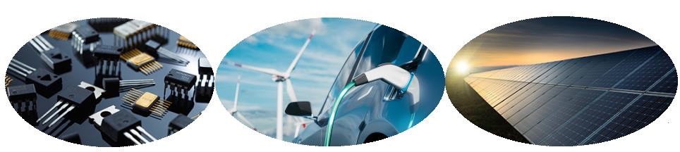
Electric Vehicles (EVs) – On-board chargers, traction inverters, DC-DC converters
Charging Stations – High-power fast charging infrastructure
Renewable Energy – Photovoltaic inverters, wind power converters
Energy Storage Systems – Grid-tied storage power conditioning
Rail Transit & Smart Grid – High-voltage traction and transmission
Industrial Power Supplies & Drives – Motor drives, UPS systems
Why Choose HMT?
Grade Options: P-grade and D-grade available for different cost-performance requirements
Manufacturer Direct: Competitive pricing with full in-house quality control
Customization: Off-axis orientation, thickness, and surface finish can be tailored
Quality Assurance: Low defect density ensures reliable epitaxial growth
Global Supply: Reliable shipping to North America, Europe, and Asia
Related Products
CATEGORIES
LATEST NEWS
- Introduction to the main functions of PbootCMS
What Is a TCB Nozzle? Materials, Vacuum Holding and SiC Nozzle Manufacturing
- Introduction to the main functions of PbootCMS
SiC : Industrial Ceramic vs Semiconductor Applications
- Introduction to the main functions of PbootCMS
How Does AI Help Singe Crystal SiC Boule Growth
- Introduction to the main functions of PbootCMS
Technical Analysis of SiC Wafer For Power Semiconductor Devices in New Energy Vehicles
CONTACT US
Contact: Mr.Kimrui
Phone:
Tel: Please send your detailed inquiry or requirements via email below.
Email: kim@homray-material.com
Add: Please send your detailed inquiry or requirements via email below.